Quantum well and III-V electronics
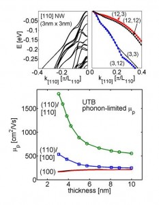
Hole Mobility in Si Ultra-Thin Layers
 Objective:
•Understand the influence of confinement length scale and confinement direction and transport orientation on carrier mobility in ultra-thin Si layers
Approach:
•Use the sp3d5s*-SO tight-binding model for electronic structure calculation and linearized Boltzmann transport theory
Results:
•The electronic structure is a strong function of geometry at the nanoscale
•For holes, the (110)/[110] channels are highly advantageous compared to other configurations
•(110) surfaces have a larger hole confinement effective mass and are more tolerant to surface roughness scattering
___________________________________________________________________________________________
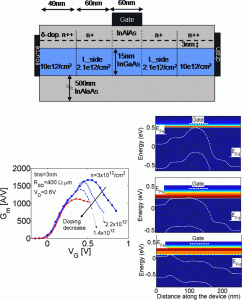
Quantum transport in III-V HEMTs for High Performance Logic Applications
 Objective:
• Understand experimental data on III-V HEMT devices for logic applications
• How close to the ballistic limit are short channel III-V devices
• What controls their performance
Approach:
• Use a 2D quantum (NEGF) simulator
• Simulate the experimental structure using delta-doped doping
• Use the sp3d5s* TB model to extract the effective mass of the III-V channel
Impact:
• Devices as short as LG=60nm are close to the ballistic limit
• The series resistance Rsd and the design of the contacts affects the performance
• Identified the low doping in the contacts as the most possible reason for the Gm degradation observed in experimental data
Result:
•Gm rolls off as the gate bias increases, possibly due to source exhaustion