Nanowire (NW) electronics
Hole Mobility in Ultra-Scaled NWs
 Objective:
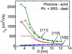
•Understand the influence of confinement length scale and confinement direction and transport orientation on the low-filed mobility of p-type Si NWs
Approach:
•Use the sp3d5s*-SO tight-binding model for electronic structure calculation and linearized Boltzmann transport theory
Results:
•The low-filed mobility is a strong function of geometry at the nanoscale
•Large mobility anisotropy is observed. [111] and [110] NWs are highly advantageous
•Mobility improves in [111] and [110] p-type NWs with diameter scaling, and the detrimental effect of surface roughness scattering can be offset
___________________________________________________________________________________________
A 2D Ballistic Atomistic Model for the Investigation of Band Structure Effects
 Objective:
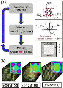
• Understand the effects of bandstructure in nanoscale nanowire devices
• Understand the effect of charge self-consistency on the dispersions
Approach:
• Use the sp3d5s*-SO atomistic TB model for the electronic structure
• Use the semi-classical ballistic top-of-the-barrier model
• Solve the 2D poisson in the cross section of the wire
• Self-consistently iterate with the bandstructure calculation model
Impact:
• Transport features in nanowires in different orientations can be explained
• Prediction for performance optimization
For a related research project, please see Band Structure Lab on nanoHUB.
___________________________________________________________________________________________
Band Structure Effects in Silicon Nanowire Electron Transport
 Objective:
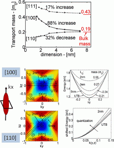
• Understand the transport properties of NMOS Si nanowire devices at the ballistic limit
• Investigate bandstructure effects in ultra-scaled Si NMOS nanowires
Approach:
• Use the sp3d5s*-SO TB atomistic model for the electronic structure calculation
• Investigate the scaling behavior and transport properties of NWs in various orientations
Results:
• The effective mass of the NWs varies as the NW is scaled, and varies differently in different orientations
• The anisotropy and non-parabolicity of the electronic structure is responsible for this behavior
___________________________________________________________________________________________
Band Structure Effects in Silicon Nanowire Hole Transport
 Objective:
• Understand the transport properties of PMOS Si nanowire devices at the ballistic limit
• Investigate bandstructure effects in ultra-scaled Si PMOS nanowires
Approach:
• Use the sp3d5s*-SO TB atomistic model for the electronic structure calculation, self-consistently coupled to a 2D Poisson
• Use a semi-classical ballistic model for transport
Results:
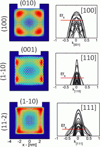
• Dispersions are different in different orientations and strongly bias dependent
• The charge placement profile is different in different oriented wires
• The capacitance of the wires and the total amount of charge is very similar
• Velocities depend on orientation and dominate the current differences
___________________________________________________________________________________________
Design for Variability: On-current Variation in [110] PMOS Nanowires
![Design for Variability: On-current Variation in [110] PMOS Nanowires Design for Variability: On-current Variation in [110] PMOS Nanowires](http://nneophytou.com/wp-content/uploads/2009/11/image52-300x179.gif) Objective:
Objective:
• Investigate mechanisms of ON-current variation by the anisotropic bandstructure
• ON-current variations at the onset of volume to surface inversion in [110] PMOS NWs
Approach:
• Use the atomistic sp3d5s*-SO model with ballistic transport
• Simulate the ON-current of devices of widths/heights 3nm-12nm (all combinations within)
• Form the ON-current variation surface
Impact:
• Design space has been identified for minimal current variations in [110] PMOS nanowires
• Sharp variations are identified at the onset of volume to surface inversion in [001] heights
• Strain can tune the sensitivity, or shift it in different regions
Results:
• The ON-current variation surface of [110] PMOS nanowires as the width in [1-10] and height in [001] is varied from 3nm to 12nm
• The charge placement is different for each quantization surface
• Sharp variations are observed at 6nm of height in [001]